
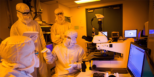
The Seattle Times reported on UW’s efforts to expand its Washington Nanofabrication Facility, a national user facility that provides UW researchers and businesses space to create tiny chips and sensors used in medical devices, electronics and vehicles.
The UW Board of Regents has allocated $37M to expand the size of the facility from 7,000 to 12,000 square feet. The expansion will break ground this November and is expected to be complete within 14 months. Karl Bohringer, joint UW professor of electrical engineering and bioengineering, is the Washington Nanofabrication Facility’s director.
The expansion will enable the facility to accommodate ever-increasing requests to use its space. Additional space will also provide room to install newer clean room technology which helps keeps harmful particles out of the air – and out of the tiny devices scientists are working on, which often involve materials smaller than the width of a human hair.
UW students and faculty can use the facility’s equipment after receiving training. Those without fabrication skills can work with facility staff to build out their designs. UW Bioengineering Associate Professor Daniel Ratner is developing a small chip to diagnose patients with blood, plasma or urine. He has the molecular engineering background needed to design the chip – but doesn’t have the manufacturing skills to fabricate it. “We’re able to lay out a sketch of the design, then submit the designs to the lab, as opposed to myself having learn to fabricate,” he said in the piece.
The facility is also open to private businesses, which pay an hourly or monthly fee to use the equipment, and can see significant cost savings compared with buying their own nanofabrication equipment or utilizing privately-held labs.
Read the story at The Seattle Times’ website